Overview
ASML is the undisputed leader in photolithography systems for semiconductor manufacturing. Its roadmap spans decades of innovation, from deep ultraviolet (DUV) tools to extreme ultraviolet (EUV) systems with progressively higher numerical aperture (NA). In 2025 alone, ASML shipped 48 EUV lithography systems and 131 immersion DUV tools, generating €32.7 billion in total revenue and ending the year with a €38.8 billion order backlog. This guide explains how ASML's technology tiers — DUV, Low-NA EUV, High-NA EUV, Hyper-NA EUV, and future concepts — form a coherent path for the chip industry. You'll learn the principles, prerequisites, step-by-step evolution, common pitfalls, and a summary of what lies ahead.

Prerequisites
To follow this guide, you should have a basic understanding of semiconductor fabrication, particularly the role of photolithography in defining transistor features. Familiarity with concepts like wavelength, resolution, and numerical aperture is helpful but not required — each term is explained. Software or hardware tools are not needed; this is a conceptual tutorial.
Step-by-Step Instructions
Step 1: Understand the DUV Foundation
Deep ultraviolet (DUV) lithography uses wavelengths of 248 nm (KrF laser) or 193 nm (ArF laser) to pattern wafers. Immersion DUV — which introduces a layer of water between the lens and wafer — pushes resolution further by effectively shortening the wavelength to 134 nm. ASML's immersion DUV tools (e.g., NXT:1980Di) remain workhorses for mature and advanced nodes. In 2025, ASML shipped 131 immersion DUV systems, confirming their ongoing demand.
Key facts:
- Wavelength: 193 nm (immersion) / 248 nm (dry)
- Resolution limit: ~38 nm half-pitch (immersion single exposure)
- Applications: Logic (28nm to 7nm), memory (DRAM, NAND), analog, power ICs
Step 2: Move to Low-NA EUV
Extreme ultraviolet (EUV) lithography uses 13.5 nm wavelength, enabling much finer resolution. ASML's first EUV generation uses a 0.33 numerical aperture (NA), often called "Low-NA EUV." These systems (TWINSCAN NXE:3400B/C) have been crucial for 7nm and 5nm nodes. The 48 EUV units shipped in 2025 include these Low-NA systems alongside some High-NA models.
Why Low-NA EUV matters:
- Resolution: ~13 nm half-pitch (single exposure)
- Throughput: Up to 160 wafers per hour (WPH)
- Limitation: For sub-3nm nodes, requires multiple exposures or design restrictions
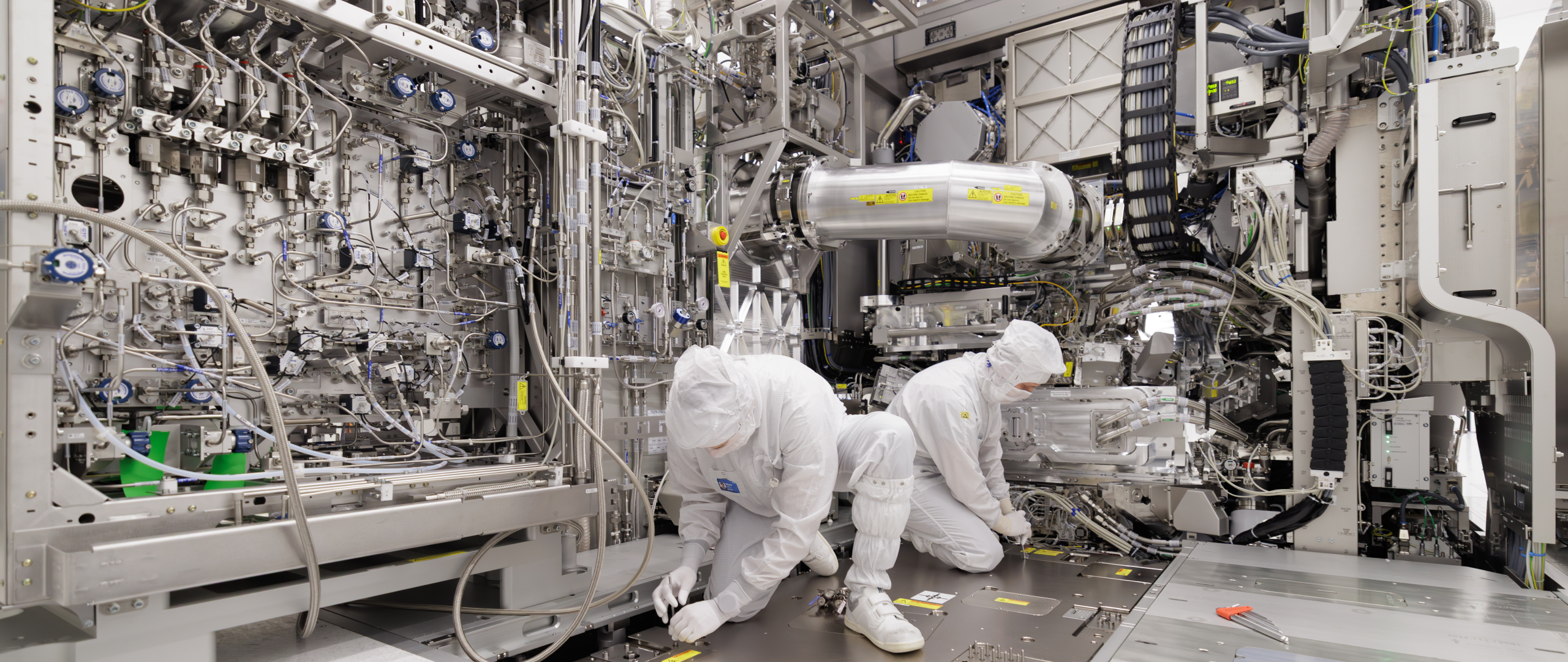
Step 3: Advance to High-NA EUV
High-NA EUV (TWINSCAN EXE:5000) increases the numerical aperture to 0.55, boosting resolution to ~8 nm half-pitch in a single exposure. This reduces the need for complex multi-patterning, lowering cost and cycle time. ASML began shipping High-NA tools in 2024, with volume ramp expected in 2025-2026. The 2025 shipment total of 48 EUV systems includes initial High-NA units.
High-NA advantages:
- Single-exposure resolution: 8 nm half-pitch
- Throughput target: 220+ WPH
- Target nodes: 2nm, 1.4nm, and 1nm (logic) for leading foundries
Step 4: Explore Hyper-NA EUV (0.7 NA and beyond)
Hyper-NA EUV is ASML's next logical step, pushing NA to 0.7 or higher. This would enable single-exposure resolution below 6 nm half-pitch, potentially extending to 0.5nm nodes. However, Hyper-NA faces significant challenges: extreme lens design, higher power requirements (sources >1 kW), and new mask materials. ASML has published conceptual roadmaps where Hyper-NA could enter production in the 2030s.
What Hyper-NA promises:
- Resolution: ~5-6 nm half-pitch single exposure
- Throughput: Potentially 250+ WPH after optimization
- Requirements: New reflective optics, higher source power, advanced pellicles
Step 5: Look Beyond EUV — Directed Self-Assembly and Other Contenders
While ASML's roadmap centers on EUV scaling, alternative technologies may complement or replace optical lithography at future nodes. Directed self-assembly (DSA) uses block copolymers to create patterns at ~5 nm pitch. Nanoimprint lithography (NIL) stamps patterns physically. However, ASML remains committed to optical solutions, with Hyper-NA expected to be the last full optical generation before possible transition to high-volume e-beam or atomic-scale processing.
Common Mistakes
Mistake 1: Confusing DUV immersion with EUV
Fact: DUV immersion uses 193 nm wavelength with water, while EUV uses 13.5 nm in vacuum. They are completely different architectures — EUV requires reflective optics, vacuum chambers, and tin plasma sources.
Mistake 2: Assuming Low-NA EUV is obsolete
Correction: Low-NA EUV remains highly relevant for many nodes. Even with High-NA available, many designs benefit from the proven reliability and lower cost per wafer of Low-NA tools. ASML's 2025 order backlog of €38.8B includes many Low-NA EUV and DUV orders.
Mistake 3: Overlooking the infrastructure required for Hyper-NA
Reality: Hyper-NA demands not just new scanners but also new masks, resists, metrology, and source development. Companies often underestimate the ecosystem investments needed.
Mistake 4: Thinking High-NA is the final step
Perspective: High-NA is a major milestone, but ASML already research Hyper-NA (0.7-0.8 NA) and possibly beyond. The roadmap extends past High-NA into the 2030s.
Summary
ASML's lithography roadmap progresses from DUV (immersion) through Low-NA EUV, High-NA EUV, Hyper-NA EUV, and eventually beyond optical lithography. Each step increases numerical aperture and reduces wavelength to achieve smaller patterns. In 2025, shipments of 48 EUV and 131 immersion DUV tools generated €32.7B revenue, with a backlog of €38.8B. Understanding these tiers helps semiconductor professionals plan for future node transitions and capital investments. The key takeaway: while High-NA is now entering high-volume manufacturing, Hyper-NA is the next frontier, and DUV will remain essential for years to come.